
Semi-Insulating SiC for RF GaN Applications
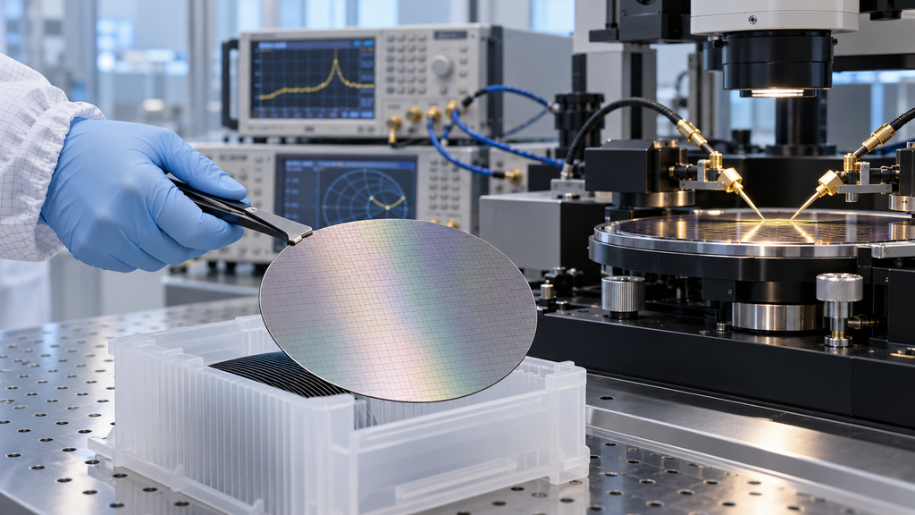
The substrate competition behind RF gallium nitride technology is becoming increasingly interesting.
In October 2026, Atomera and IQE announced a joint development program targeting RF GaN-on-silicon, while Guerrilla RF also began sampling new high-power GaN-on-SiC devices for commercial, aerospace and defense applications. The two developments illustrate an important trend: RF GaN manufacturers are actively evaluating different substrate platforms as they balance performance, thermal management and manufacturing cost.
Within this market, semi-insulating silicon carbide remains one of the most important substrate materials for high-performance RF GaN devices.
Why RF GaN Needs a Semi-Insulating Substrate
A conventional conductive semiconductor substrate can introduce unwanted electrical losses when RF devices operate at high frequencies.
For RF applications, the substrate ideally needs to provide a high-resistivity electrical foundation beneath the active GaN layers.
Semi-insulating SiC offers very high electrical resistivity while retaining the excellent thermal and mechanical properties associated with silicon carbide.
This combination is particularly valuable for high-power RF devices.
A GaN HEMT can generate considerable heat in a very small active area. If that heat is not removed efficiently, device performance, reliability and output power can decline.
SiC provides a much better thermal path than many conventional insulating substrates while maintaining electrical isolation.
This is one of the main reasons GaN-on-SiC remains important in demanding RF applications.
HPSI SiC vs Vanadium-Doped SiC
Semi-insulating SiC wafers are generally divided into two broad categories.
The first is high-purity semi-insulating SiC, commonly known as HPSI SiC.
The second uses compensation dopants such as vanadium to achieve high resistivity.
HPSI material is designed to achieve semi-insulating behavior through high material purity and carefully controlled intrinsic defects rather than relying primarily on intentional vanadium compensation.
For demanding RF applications, HPSI SiC is often preferred because lower impurity concentrations can reduce unwanted electrical and optical effects.
Vanadium-doped SiC can still be useful for many research and electronic applications, but customers should not assume that the two materials are identical simply because both are described as semi-insulating.
When specifying material, it is therefore advisable to clearly state whether HPSI or V-doped SiC is required.
Why 4-Inch HPSI SiC Still Has Demand
The semiconductor industry is steadily moving toward larger wafer diameters, but 4-inch semi-insulating SiC remains widely used.
There are several reasons.
Many research laboratories, universities and pilot production lines still operate equipment designed around 100 mm wafers.
RF device development also does not always require the largest available substrate.
A 4-inch HPSI SiC wafer can offer a practical combination of material quality, available processing equipment and manageable development cost.
For GaN epitaxy research, microwave devices, photonics and university R&D, the 4-inch format therefore remains commercially relevant.
This also explains why searches for terms such as “4 inch semi-insulating silicon carbide wafer” continue to appear in semiconductor material sourcing.
Key Properties of Semi-Insulating SiC
When selecting an RF-grade SiC substrate, resistivity is only one parameter.
Several material characteristics can influence downstream processing.
Resistivity
High resistivity reduces RF losses through the substrate.
The required value depends on the device design and operating frequency, but RF applications generally require material that remains strongly semi-insulating under actual operating conditions.
Thermal Conductivity
Thermal conductivity is one of SiC’s strongest advantages.
High-power GaN RF devices can generate substantial heat, particularly at the channel and gate region.
Efficient transfer of heat from the GaN epitaxial structure through the SiC substrate helps control junction temperature.
Crystal Quality
Micropipes, threading dislocations and other crystal defects can influence epitaxial growth and device yield.
For demanding applications, buyers should consider crystal-defect specifications rather than selecting the wafer only by diameter and resistivity.
Surface Quality
GaN epitaxy requires a carefully prepared SiC surface.
Scratches, subsurface damage and polishing defects can affect the nucleation and growth of the epitaxial layers.
A low-roughness CMP surface is therefore normally required.
Why GaN-on-SiC Still Matters
GaN can be grown on several substrate materials, including silicon, sapphire and SiC.
Silicon has a major economic advantage because large-diameter substrates and semiconductor processing infrastructure are readily available.
This is why companies continue to develop GaN-on-silicon technology for RF and power applications.
However, high-performance RF devices frequently prioritize output power and thermal performance over the lowest possible substrate cost.
In these applications, GaN-on-SiC can remain attractive.
The October 2026 sampling of new GaN-on-SiC devices by Guerrilla RF is a recent example. The devices target broadband, commercial, aerospace and defense applications, demonstrating that the GaN-on-SiC platform remains active in high-power RF development.
Meanwhile, the Atomera-IQE collaboration on RF GaN-on-silicon highlights the opposite side of the market: manufacturers are working to improve silicon-based platforms so they can compete in more performance-sensitive applications.
The market is therefore unlikely to be defined by a single substrate.
Different applications will select different materials.
Typical Applications
Semi-insulating SiC is particularly relevant to:
- RF GaN HEMTs
- Microwave power amplifiers
- Radar systems
- Satellite communications
- Base-station RF equipment
- Electronic warfare systems
- Tactical communications
- High-frequency research devices
- Photonics and quantum-device research
Defense and aerospace applications are especially attractive for GaN-on-SiC because performance, temperature capability and reliability often outweigh substrate cost.
Important Wafer Specifications
A typical semi-insulating SiC RFQ should specify:
Polytype: 4H-SiC
Diameter: 2 inch, 3 inch, 4 inch, 6 inch or larger
Electrical Type: Semi-insulating
Grade: HPSI or V-doped
Orientation: On-axis or specified off-axis orientation
Thickness: According to process requirements
Surface: Si-face CMP polished
Polishing: SSP or DSP
TTV: Defined according to wafer diameter
Bow / Warp: Important for epitaxy and automated handling
Surface Roughness: Typically controlled by AFM measurement
Defect Requirements: Micropipes and crystallographic defects as required
If GaN epitaxy will be performed, customers should also discuss the substrate specifications with their epitaxy provider.
SSP or DSP?
Many GaN epitaxy processes only require a high-quality polished front surface.
In this case, single-side-polished material can be sufficient.
Double-side-polished SiC may be selected when backside optical inspection, bonding, precise thickness control or specialized device processing is required.
DSP should therefore be selected according to the actual process rather than simply assuming that it represents a higher grade.
Substrate Choice Will Become More Application-Specific
The latest RF GaN developments show that substrate technology remains highly competitive.
GaN-on-silicon is advancing because of its potential cost and manufacturing advantages.
GaN-on-SiC continues to offer strong thermal performance and is well suited to demanding high-power RF applications.
For substrate suppliers, this means semi-insulating SiC remains an important specialized market even as mainstream SiC power electronics move toward larger conductive wafers.
For engineers and procurement teams, the most important step is to define the intended RF application before specifying the wafer.
A well-selected semi-insulating SiC substrate provides more than electrical isolation. It forms the thermal, mechanical and crystalline foundation of the complete RF GaN device.
Discuss a material requirement
Send specifications or a drawing to our materials team.