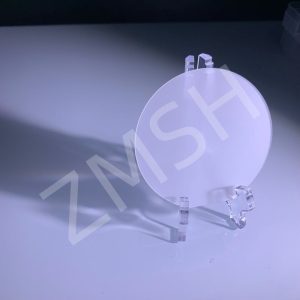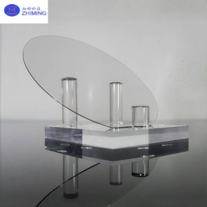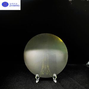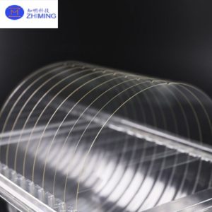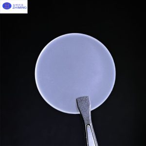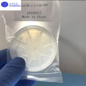
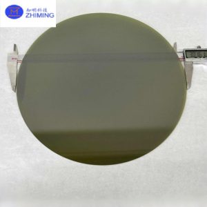
12-Inch 300 mm 4H-SiC Wafer, 750 ± 25 μm
Large-diameter silicon carbide wafer based on the reference listing for 300 mm / 12-inch research-grade substrates. Polytype, conductivity, orientation, thickness, resistivity, defect…
View specifications →Browse semiconductor materials and precision components. Use the inquiry form at the bottom of each category page to send your requirements.
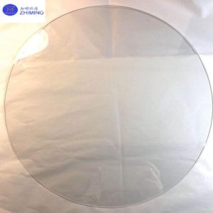
Large-diameter silicon carbide wafer based on the reference listing for 300 mm / 12-inch research-grade substrates. Polytype, conductivity, orientation, thickness, resistivity, defect…
View specifications →
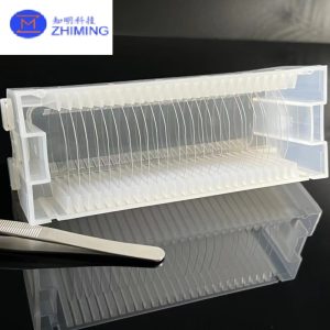
Large-diameter monocrystalline Al2O3 sapphire wafer for LED, optoelectronic, and semiconductor development. Reference listing describes a 12-inch format with DSP/SSP and multiple crystal-plane…
View specifications →
Single-crystal Al2O3 wafer listed for LED, semiconductor, and optical applications. Confirm diameter tolerance, thickness, orientation, polish side, and surface condition against the…
View specifications →
Monocrystalline Al2O3 sapphire wafer for semiconductor and optical development. The reference listing shows a 4-inch C-plane format with double-side or single-side polishing…
View specifications →
High-purity semi-insulating silicon carbide wafer listed in a 4-inch, 350 μm example for AR-glass and semiconductor development. Confirm resistivity, polytype, surface finish,…
View specifications →
8-inch SiC epitaxial wafer option for power-device and semiconductor development. Specify substrate polytype, conductivity, epi stack, layer thickness, doping, and inspection requirements.
View specifications →
BF33 borosilicate glass substrate listed for semiconductor, MEMS, and optical applications. Specify wafer size, thickness, surface finish, edge profile, and bonding or…
View specifications →
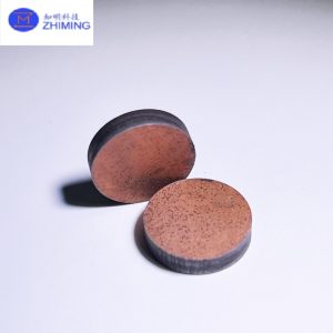
Diamond-copper composite option for high-thermal-conductivity and tailored-expansion designs. Specify composite architecture, dimensions, target thermal performance, test method, and interface requirements.
View specifications →
Quartz plate option listed with one side frosted and one side polished for optical and semiconductor applications. Define material grade, dimensions, thickness,…
View specifications →
GaN epitaxy template on sapphire listed in 2-, 4-, 6-, and 8-inch formats. Specify wafer diameter, sapphire orientation, GaN/AlN layer structure, thickness,…
View specifications →
Sapphire crystal blank for downstream wafering, optical fabrication, and precision component machining. Provide target geometry, crystal orientation, and machining allowance for review.
View specifications →
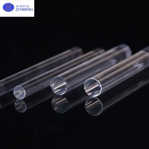
Quartz tube options for semiconductor and industrial equipment. Specify inner and outer diameters, wall thickness, length, end geometry, material grade, and operating…
View specifications →
High-temperature quartz boat and carrier options for semiconductor wafer processing. Provide wafer diameter, slot count, pitch, dimensions, process temperature, and cleaning requirements.
View specifications →
Custom sapphire watch cases for watch brands and component manufacturers. Shape, openings, finishing, and assembly interfaces are made to approved drawings.
View specifications →
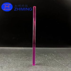
Synthetic ruby rods for laser, optical, and instrument applications. Diameter, length, end-face finish, and coating requirements can be reviewed from drawings.
View specifications →Share your material, dimensions, tolerances, quantity, and target date. Our team will review the requirements and respond.