BF33 Glass Wafers for MEMS Bonding
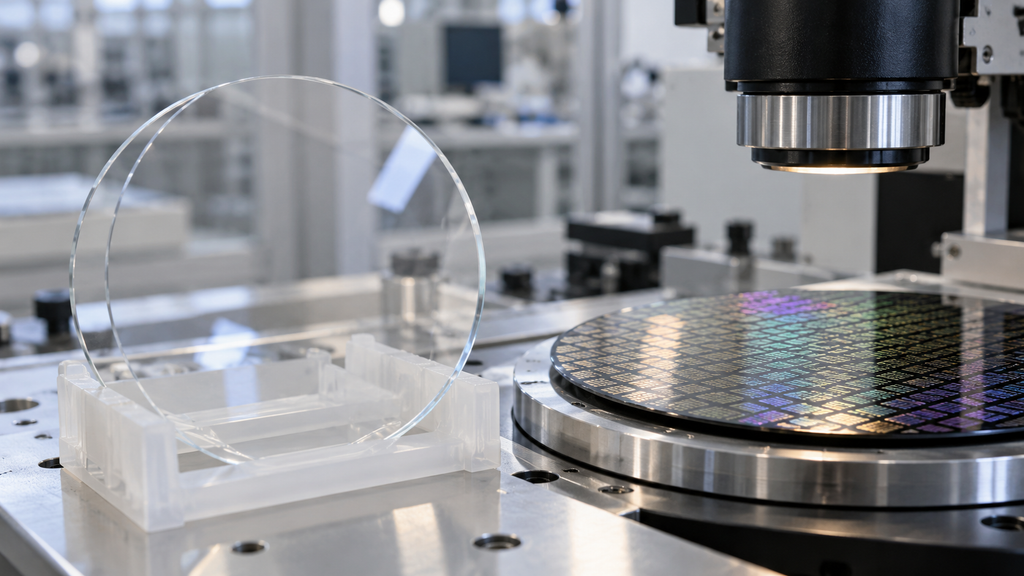
Borosilicate glass remains one of the most useful substrate materials in MEMS manufacturing.
While advanced semiconductor packaging has recently increased interest in glass substrates, materials such as BF33 borosilicate glass have already been used for many years in MEMS, sensors, microfluidics and wafer-level bonding.
Recent research continues to improve wafer-level bonding technologies. A 2026 study demonstrated an ALD-alumina-enabled anodic bonding approach for integrating different functional substrates in MEMS structures, highlighting continued development around low-temperature and hermetic wafer bonding.
For engineers selecting glass substrates, however, the fundamental requirements remain closely connected to material composition, thermal expansion, flatness and surface quality.
What Is BF33 Glass?
BF33 is a borosilicate glass material designed for applications requiring good thermal stability, chemical resistance and dimensional control.
Its properties make it suitable for semiconductor and MEMS manufacturing where ordinary soda-lime glass may not provide sufficient process stability.
BF33 glass wafers can be supplied in semiconductor-compatible wafer formats and processed using techniques such as:
- Mechanical polishing
- Laser drilling
- Wet etching
- Thin-film deposition
- Metallization
- Wafer bonding
- Precision dicing
The material is particularly useful where optical transparency and electrical insulation are required simultaneously.
Why MEMS Uses Glass Wafers
Many MEMS devices contain moving structures or cavities.
These structures often need to be protected from contamination, moisture or atmospheric pressure.
A glass cap wafer can be bonded to the silicon device wafer to create a sealed cavity.
Because glass is transparent, it also provides several manufacturing advantages.
Engineers can inspect alignment and structures through the cap wafer.
This is particularly useful for:
- Pressure sensors
- Microfluidic devices
- Optical MEMS
- MEMS microphones
- Inertial sensors
- Lab-on-chip devices
Glass can therefore serve as both a structural packaging material and an optical interface.
The Importance of Thermal Expansion
One of the most important considerations in silicon-glass bonding is coefficient of thermal expansion.
When two different materials are heated during bonding and then cooled, they contract at different rates.
A large CTE mismatch creates mechanical stress.
This stress can cause:
- Wafer bow
- Bonding failure
- Cracking
- Device deformation
- Reliability problems
Borosilicate glasses are attractive because their thermal expansion can be relatively compatible with silicon across appropriate process temperature ranges.
This is one reason they are frequently used in anodic bonding.
What Is Anodic Bonding?
Anodic bonding is a common method for joining silicon and glass.
The process generally applies elevated temperature together with a high electrical potential.
Mobile ions inside the glass migrate under the electric field, allowing a strong chemical bond to form near the silicon-glass interface.
The result can be a strong and hermetic wafer-level bond without the need for an adhesive layer.
This process is widely used for MEMS packaging.
A 2026 study of anodic bonding for heterogeneous MEMS integration also demonstrates that researchers continue to explore new intermediate layers and process conditions to reduce thermal budgets and integrate more complex substrate combinations.
Surface Roughness Matters
Good wafer bonding depends strongly on the condition of the two surfaces.
If surface roughness is too high, the wafers cannot form uniform intimate contact.
Local gaps can become bonding voids.
For this reason, BF33 wafers intended for bonding commonly require carefully polished surfaces.
The required roughness depends on the specific bonding process, but it is important to define measurement method and wafer side.
For some MEMS processes, only one side requires precision polishing.
For others, double-side polishing provides advantages for alignment and optical inspection.
TTV, Bow and Warp
Surface roughness alone does not determine bonding performance.
Wafer geometry is equally important.
Total Thickness Variation
TTV represents thickness variation across the wafer.
Excessive TTV can create non-uniform contact pressure and complicate lithography or bonding.
Bow
Bow describes the overall curvature of the wafer relative to a reference plane.
Warp
Warp captures more complex wafer deformation.
Large bow or warp can prevent uniform contact during bonding.
As wafer diameter increases, controlling these parameters becomes more challenging.
Customers should therefore specify acceptable geometry rather than ordering glass only by nominal thickness.
BF33 for Microfluidics
Borosilicate glass is also widely used in microfluidic systems.
Glass offers:
- Chemical resistance
- Optical transparency
- Electrical insulation
- Smooth channel surfaces
- Good dimensional stability
Microchannels can be produced using wet etching, laser processing or other micromachining techniques.
A second glass or silicon wafer can then be bonded over the patterned surface.
Applications include biomedical analysis, chemical sensing and lab-on-chip systems.
Optical Advantages
Unlike silicon, BF33 is transparent through a broad visible range.
This allows inspection of structures beneath the glass.
For optical sensors or microfluidics, transparency can also form part of the final device function.
However, customers should distinguish between standard semiconductor-polished glass and high-end optical substrates.
If the application requires precision optical performance, additional specifications such as transmitted wavefront, parallelism and cosmetic quality may be needed.
Holes and Cavities in Glass
MEMS glass wafers often require customized features.
Examples include:
- Through holes
- Fluid ports
- Electrical feedthrough openings
- Cavities
- Alignment marks
- Laser-drilled vias
The manufacturing process should be selected based on hole diameter, wafer thickness and required edge quality.
Laser processing provides flexibility and speed, while wet etching can provide different wall profiles and surface characteristics.
Customers should define both the nominal dimensions and tolerances.
Edge Quality Is Often Overlooked
Glass is brittle.
Edge chips or microcracks introduced during cutting and grinding can reduce mechanical strength.
This becomes increasingly important during high-temperature bonding or vacuum processing.
A semiconductor-grade glass wafer should therefore include a controlled edge profile.
Typical options may include chamfered or rounded edges.
Proper edge processing also reduces particle generation during handling.
SSP or DSP BF33?
Single-side-polished BF33 can be sufficient when only one side participates in bonding or device fabrication.
Double-side-polished material is useful when:
- Both sides require lithography
- Optical transmission is important
- Backside alignment is required
- Both surfaces will be bonded
- Precision inspection is required
As with semiconductor wafers, DSP should not automatically be selected simply because it appears more advanced.
The process should determine the polishing configuration.
What to Specify in an RFQ
A useful BF33 glass wafer request should include:
Material: BF33 or equivalent specified borosilicate glass
Diameter: For example 2, 4, 6 or 8 inch
Thickness: According to device design
Thickness Tolerance: Clearly defined
TTV: Particularly important for bonding
Bow / Warp: According to process requirements
Surface: SSP or DSP
Surface Roughness: Specify measurement requirement
Edge Profile: Chamfer or other required geometry
Custom Features: Holes, cavities or patterns
Cleaning: Semiconductor-compatible cleaning if required
Packaging: Cleanroom-compatible packaging where applicable
If the wafer will be bonded to silicon, the intended bonding method and temperature should also be included.
BF33 Remains a Practical MEMS Material
Interest in next-generation semiconductor glass substrates is increasing, but traditional borosilicate glass wafers remain highly relevant.
Their value comes from a practical combination of transparency, electrical insulation, thermal stability and compatibility with wafer bonding.
For MEMS engineers, the most important consideration is not simply whether the material is called BF33.
The success of the process depends on matching the glass composition, wafer geometry, surface finish and bonding conditions to the device.
As MEMS, sensors and microfluidic devices become more integrated, well-controlled borosilicate glass substrates will continue to play an important role in wafer-level manufacturing.
Discuss a material requirement
Send specifications or a drawing to our materials team.