
Selecting a SiC Wafer for Power Device Development
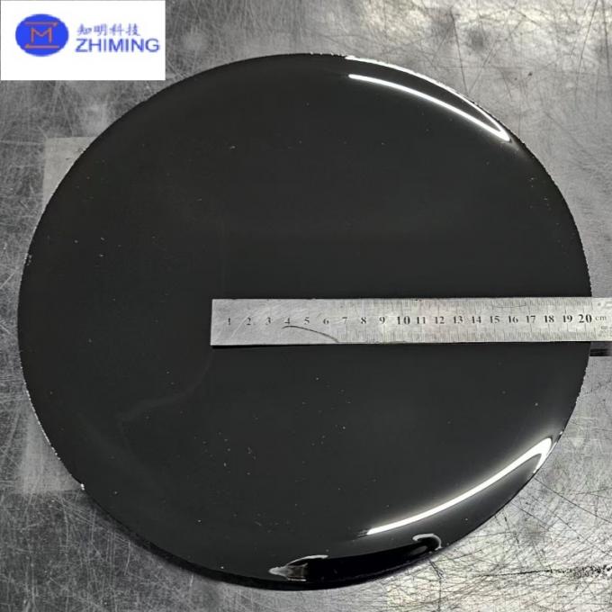
Silicon carbide wafer selection should begin with the device structure and process flow. A wafer that appears suitable by diameter alone may still differ in polytype, conductivity, orientation, thickness, surface finish, or defect criteria.
Start with the device and process
For power device development, define whether the project requires a conductive or semi-insulating substrate, the intended epitaxial layer, and the target device architecture. Confirm wafer diameter and thickness against the tool set and handling system. The exact orientation and off-angle should follow the epitaxy or device process requirements rather than a generic catalog default.
Confirm surface and defect requirements
Clarify whether the incoming wafer is epi-ready or intended for another process. Specify polish side, roughness method, total thickness variation, bow and warp limits, edge profile, and any defect screening such as micropipe or basal-plane dislocation limits. Agree on the inspection method and report format before ordering.
Prepare a complete request
A useful request includes polytype, conductivity or resistivity, diameter, orientation, thickness, surface condition, quantity, and target date. For development lots, identify which parameters are fixed and which may be adjusted after process evaluation.
Discuss a material requirement
Send specifications or a drawing to our materials team.