
How to Specify Sapphire Substrates for Optical and Semiconductor Use
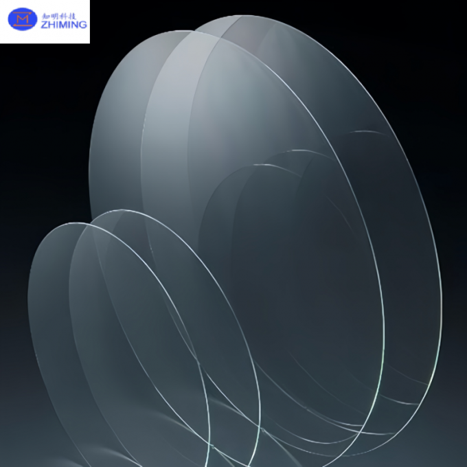
Sapphire substrates are used in applications ranging from epitaxy and photonics to optical protection and sensing. The correct specification depends on whether the substrate is serving as a growth platform, a transparent optical element, or a machined component.
Separate material from geometry
State crystal orientation, diameter or overall dimensions, thickness, and any off-angle requirement. For wafer use, add polish side, flatness or TTV requirements, edge profile, and packaging. For an optical component, include clear aperture, wavelength range, transmission target, surface quality, flatness, parallelism, and coating requirement.
Describe the use environment
Thermal cycling, chemical exposure, mounting stress, and cleaning method can influence material and geometry choices. Include these conditions in the inquiry, especially for windows and custom shapes.
Align inspection with function
Request inspection points that can be measured and tied to the drawing. If coating or optical performance is required, define the measurement band, angle, and acceptance method. Confirm the agreed records and packaging before production.
Discuss a material requirement
Send specifications or a drawing to our materials team.