
BF33 Glass Wafers for MEMS, Sensors and Optical Development
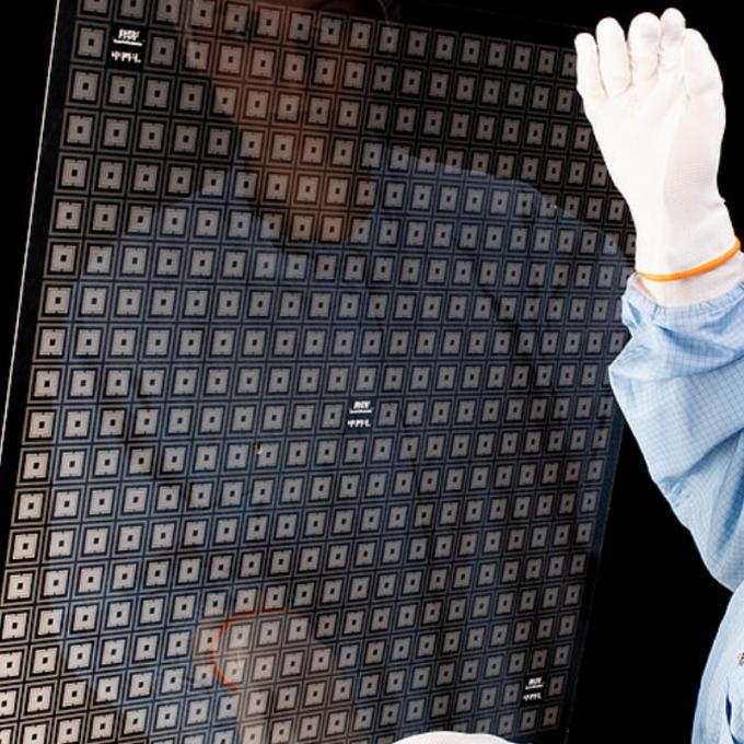
BF33 borosilicate glass wafers are considered for projects that need a glass substrate with controlled geometry and a defined process interface. Application suitability depends on the device stack, bonding method, thermal cycle, and optical or mechanical requirements.
Specify the wafer format
Include diameter, thickness, tolerance, orientation or cut, edge profile, and surface finish. If the wafer will be bonded, state the mating material and process. For optical use, describe the wavelength range, transmission target, surface quality, flatness, and any coating requirements.
Connect the material to the process
MEMS and sensor flows may include patterning, bonding, drilling, dicing, or thermal cycling. Share which steps the glass must tolerate and whether the wafer is needed as a carrier, cap, cover, or functional substrate.
Plan incoming acceptance
Identify critical dimensions, visual criteria, cleaning, and packaging. A clear acceptance checklist lets the sample stage verify the substrate before a larger lot is scheduled.
Discuss a material requirement
Send specifications or a drawing to our materials team.