
6 Inch SiC As-Cut Wafer for Substrate Processing and Equipment Validation
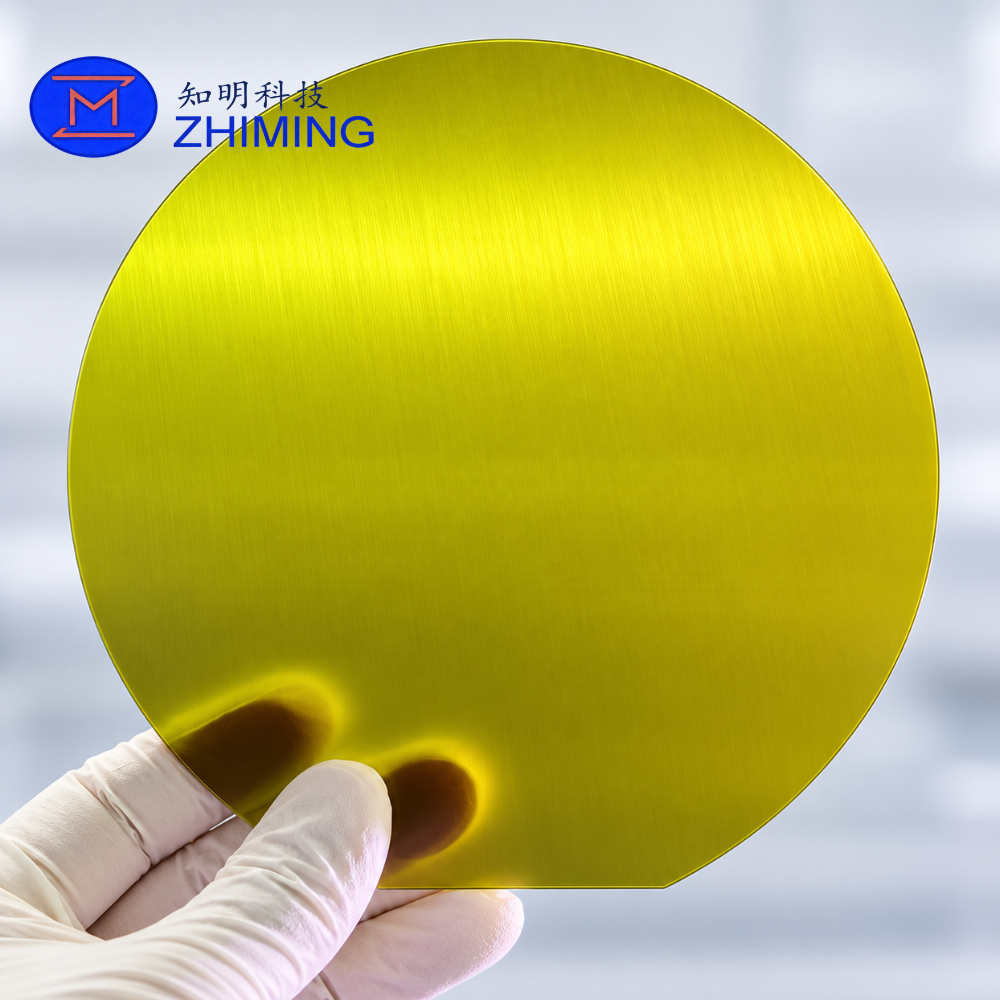
The 6 Inch SiC As-Cut Wafer is supplied at an early stage of silicon carbide wafer processing, directly after slicing from a SiC crystal boule.
Unlike polished or epi-ready substrates, this product does not undergo final grinding, lapping, polishing, or CMP finishing before delivery. The original sliced surface is retained, making it suitable for customers who need real SiC material for downstream processing, machine testing, process qualification, or manufacturing development.
This type of wafer is widely used where polished semiconductor-grade surface quality is not required.
 Product Highlights
- 6 inch / 150 mm SiC wafer format
- Supplied in as-cut condition
- Unpolished wafer surface
- Suitable for further grinding and lapping
- Ideal for polishing and CMP process development
- Useful for equipment validation and process setup
- Custom thickness and material specifications available
- Suitable for laboratory and industrial use
- Cost-efficient solution for process testing
Standard Product Information
| Parameter | Description |
|---|---|
| Material | Silicon Carbide (SiC) |
| Diameter | 6 Inch / 150 mm |
| Product Condition | As-Cut |
| Surface | Unpolished |
| Crystal Structure | 4H-SiC / 6H-SiC / Optional |
| Conductivity | N-Type / Semi-Insulating / Optional |
| Orientation | Standard or Customized |
| Thickness | Customized |
| Edge Type | Flat / Notch / Customized |
| Further Processing | Available Upon Request |
| Supply Quantity | Prototype, Small Batch, Volume |
Specifications can be adjusted according to customer application.
 As-Cut Surface Characteristics
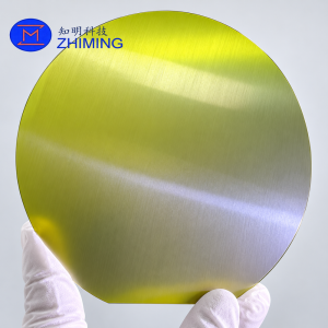
The as-cut surface is the original wafer surface obtained after slicing the SiC crystal.
Typical characteristics may include:
- Visible cutting traces
- Directional saw marks
- Matte or semi-matte appearance
- Relatively high surface roughness
- No final polishing
- No CMP finish
These are normal characteristics of raw SiC wafers and are suitable for customers performing their own downstream wafer processing.
Typical Processing Flow
A silicon carbide substrate usually passes through several manufacturing stages:
SiC Crystal Boule → Slicing → Grinding → Lapping → Polishing → CMP → Cleaning → Finished Substrate
The 6 inch SiC as-cut wafer is supplied immediately after the slicing stage.
This gives customers greater flexibility to develop or control their own downstream processing.
Main Applications
 SiC Wafer Grinding
Used to evaluate wafer grinding equipment, grinding wheels, process parameters, removal rates, and final thickness control.
Wafer Lapping
Suitable for studying lapping performance, abrasive selection, flatness improvement, and surface damage removal.
Polishing Process Development
Can be used for mechanical polishing, pre-polishing, and CMP process experiments.
Semiconductor Equipment Qualification
Suitable for machine setup and functional verification of:
- Wafer grinders
- Lapping machines
- Polishing machines
- Wafer thinning equipment
- Wafer handling systems
- Robot transfer systems
- Cleaning and inspection equipment
R&D Testing
Suitable for material science research, SiC machining studies, surface treatment research, and process optimization.
Dummy Wafer Use
For applications that do not require electronic-grade or epi-ready wafers, as-cut SiC wafers can be used as test or dummy substrates.
Advantages for Process Development
Lower Testing Cost
Using fully polished or epi-ready SiC substrates for equipment trials can increase development costs.
As-cut wafers provide actual silicon carbide material at an earlier manufacturing stage, making them more suitable for process development.
Real SiC Material Behavior
Compared with substitute materials, real SiC wafers provide more representative data for:
- Material removal
- Tool wear
- Grinding force
- Surface damage
- Polishing efficiency
- Wafer handling
Flexible Customization
Different thicknesses and material configurations can be supplied depending on the customer’s equipment or research requirements.
Available Custom Options
We can discuss customized requirements including:
- 4H-SiC or 6H-SiC
- N-Type or Semi-Insulating
- Wafer thickness
- Thickness tolerance
- Crystal orientation
- Off-axis angle
- Flat or notch design
- Edge treatment
- Grinding
- Lapping
- Single-side polishing
- Double-side polishing
- CMP
- Special test wafer requirements
Available Surface Conditions
Customers can select different processing stages based on application:
As-Cut SiC Wafer
For raw material processing and equipment testing.
Ground SiC Wafer
For improved thickness uniformity.
Lapped SiC Wafer
For intermediate processing requirements.
SSP SiC Wafer
Single-side polished.
DSP SiC Wafer
Double-side polished.
CMP SiC Wafer
For applications requiring high-quality polished surfaces.
Suitable Customers
This product is suitable for:
- Semiconductor equipment manufacturers
- SiC wafer manufacturers
- Grinding and polishing companies
- CMP technology developers
- Research laboratories
- Universities
- Material processing companies
- Wafer thinning companies
- Abrasive manufacturers
- Semiconductor process development teams
Quality and Supply Support
Each order can be supplied according to agreed technical specifications.
Before production or shipment, parameters such as diameter, thickness, surface condition, wafer type, orientation, and quantity can be confirmed according to customer requirements.
Technical documents or inspection data can also be discussed based on order specifications.
RFQ Information
To receive an accurate quotation, please provide:
- Diameter
- Thickness
- Quantity
- Crystal type
- Conductivity
- Orientation
- Surface condition
- Flat or notch requirement
- Application
- Required tolerances
If some parameters are not confirmed, please tell us the intended application and we can recommend a suitable configuration.
Discuss a material requirement
Send specifications or a drawing to our materials team.