
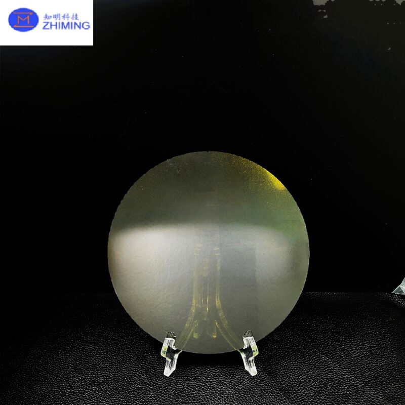
8-Inch Silicon Carbide Epitaxial Wafer
Product overview
An 8-inch silicon carbide epitaxial wafer option for power-device development and process qualification. Epitaxial requirements vary by device design: please specify the substrate type, polytype, conductivity, epitaxial layer structure, thickness, doping or resistivity target, defect criteria, and measurement method. Confirm the exact product configuration with the supplier before quotation.
Application areas
Typical project discussions include power-device substrates, RF device development, epitaxial growth, and high-temperature electronics.
Specification options
The following details can be reviewed for this product:
- 8-inch nominal format listed
- Silicon carbide epitaxial wafer
- Polytype and substrate conductivity by confirmation
- Epi layer structure, thickness and doping by drawing
- Surface and defect criteria by agreement
- Inspection report requirements by agreement
What to include in your inquiry
Please send the required dimensions, material grade or type, tolerance, surface condition, quantity, intended application, and target delivery date. A drawing or inspection checklist is helpful for custom geometries.
Availability and quality confirmation
Custom specification; lead time confirmed per lot Inspection points and document format should be agreed before order confirmation; no unverified stock or certification claim is implied.
Discuss a material requirement
Send specifications or a drawing to our materials team.