
SSP vs DSP Wafers for Bonding and MEMS
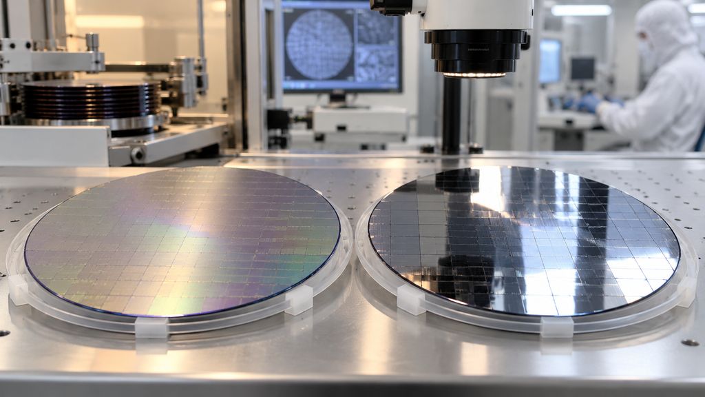
Choosing between a single-side-polished wafer and a double-side-polished wafer may appear simple, but the decision can have a major influence on semiconductor processing.
As wafer bonding, MEMS and heterogeneous integration become more sophisticated, the backside of a wafer increasingly matters.
In 2026, wafer bonding technology continues to advance rapidly. Imec and EV Group demonstrated wafer-to-wafer hybrid bonding with a 200 nm copper interconnect pitch in May, while Applied Materials and Besi expanded their bonding collaboration in October to cover additional die-to-wafer, die-to-die and die-to-panel architectures.
These developments are focused on advanced devices, but they highlight a broader materials principle:
surface quality on both sides of a substrate is becoming more important in many semiconductor processes.
What Is an SSP Wafer?
SSP means single-side polished.
Only one side of the substrate receives a high-quality polishing process.
The opposite side may remain lapped, ground or finished to a less demanding specification.
The polished surface normally becomes the device side.
SSP wafers are widely used because many semiconductor processes only require one high-quality surface.
Typical applications include:
- Epitaxial growth
- Basic thin-film deposition
- Research substrates
- Front-side lithography
- Power semiconductor development
- General material testing
Because only one surface requires precision polishing, SSP wafers can often be produced more economically.
What Is a DSP Wafer?
DSP means double-side polished.
Both surfaces are processed to achieve low roughness and controlled surface quality.
DSP wafers are often used when the backside must participate in processing, inspection or optical transmission.
Typical applications include:
- MEMS
- Wafer bonding
- Backside lithography
- Through-wafer processing
- Optical substrates
- Double-sided alignment
- Wafer-level packaging
- Precision thickness applications
The extra polishing step usually increases cost, but it can provide significant process advantages.
Why MEMS Often Requires DSP
MEMS devices frequently use both sides of a wafer.
A sensor structure may be patterned on the front while cavities, vias or alignment structures are created from the backside.
If backside lithography is required, a rough surface can reduce alignment accuracy and photoresist uniformity.
DSP wafers therefore provide a more controlled platform.
Examples include:
- Pressure sensors
- Accelerometers
- Gyroscopes
- Microfluidic devices
- MEMS microphones
- Optical MEMS
In wafer-level MEMS packaging, the substrate may also need to be bonded to a cap wafer.
Both surface flatness and cleanliness become important.
Wafer Bonding Changes the Requirements
Wafer bonding places much greater demands on surface condition than conventional wafer handling.
Two surfaces must approach each other closely enough to form a stable interface.
Particles, surface roughness or wafer deformation can create local gaps and bonding voids.
Depending on the process, bonding methods include:
- Anodic bonding
- Fusion bonding
- Direct bonding
- Adhesive bonding
- Metal bonding
- Hybrid bonding
Each process has different surface requirements.
For example, direct bonding typically requires extremely smooth and clean surfaces.
Anodic bonding between silicon and glass can tolerate a different process window but still requires controlled flatness and surface condition.
DSP Does Not Automatically Mean Better Flatness
One common misunderstanding is that DSP automatically guarantees lower TTV, bow and warp.
It does not.
Polishing configuration and wafer geometry are related, but they are separate specifications.
A DSP wafer can still have unacceptable TTV or warp.
Likewise, a carefully manufactured SSP wafer can have excellent geometry.
For precision applications, customers should specify:
- Thickness
- Thickness tolerance
- TTV
- Bow
- Warp
- Surface roughness
rather than relying only on the terms SSP or DSP.
Optical Applications Favor DSP
Transparent materials frequently require two polished surfaces.
For example:
- Sapphire
- Fused silica
- Quartz
- Borosilicate glass
A rough backside scatters light.
If the wafer will be used as an optical window, sensor cover or optical substrate, the rear surface normally needs to be polished.
DSP can therefore improve transmission and reduce scattering.
However, semiconductor-grade DSP and optical-grade polishing should not be treated as identical specifications.
An optical substrate may also require:
- Surface flatness
- Parallelism
- Scratch-dig control
- Transmitted wavefront requirements
- Optical coatings
SSP for Epitaxy
For many epitaxial processes, only one side needs an atomically smooth surface.
Examples include SiC substrates used for GaN or SiC epitaxy.
The front surface may receive CMP processing while the backside remains mechanically polished or lapped.
In these cases, SSP can reduce cost without negatively affecting the epitaxial layer.
The important question is whether backside condition affects wafer chucking, thermal contact or automated handling.
If it does, a more controlled backside finish may still be necessary.
DSP for Backside Alignment
Some semiconductor processes expose or align features from both sides of the substrate.
MEMS is a common example.
Transparent substrates can simplify alignment, but silicon wafers may require infrared alignment systems.
A polished backside improves optical access and reduces scattering.
As structures become smaller, backside surface quality can therefore affect process accuracy.
Material Makes a Difference
The cost difference between SSP and DSP depends strongly on the substrate material.
Silicon
Silicon polishing is highly mature and can achieve extremely low surface roughness.
Silicon Carbide
SiC is much harder than silicon and requires more intensive grinding and CMP.
Double-side polishing therefore adds significant processing time.
Sapphire
Sapphire is also extremely hard and anisotropic.
The required polish depends on crystal orientation and application.
Glass
Borosilicate and fused silica wafers can be polished on both sides for bonding, optical and MEMS applications.
Glass thickness and flatness should be controlled carefully when bonding to silicon.
How to Choose SSP or DSP
A simple rule is:
Choose SSP when only one surface participates in the critical process.
Choose DSP when both surfaces influence device fabrication, bonding, alignment or optical performance.
For a typical semiconductor epitaxy project, SSP may be sufficient.
For wafer bonding or MEMS, DSP is often preferred.
For transparent optical substrates, DSP is commonly required.
Questions to Ask Before Ordering
Before specifying the polishing configuration, consider:
Will the backside be patterned?
Will the wafer be bonded?
Is backside alignment required?
Will light pass through the substrate?
Will the backside contact a precision vacuum chuck?
Will the wafer be thinned later?
Is surface roughness specified on both sides?
Does the application require low TTV or low warp?
Answering these questions normally makes the SSP/DSP decision straightforward.
SSP vs DSP Is a Process Decision
There is no universal answer to whether SSP or DSP is better.
A more expensive double-side-polished wafer does not automatically improve every process.
The correct wafer is the one whose surface configuration matches the manufacturing sequence.
As semiconductor manufacturing incorporates more wafer bonding, MEMS integration and 3D structures, backside quality is receiving more attention.
That makes polishing configuration an increasingly important part of substrate selection.
For procurement teams, specifying SSP or DSP together with roughness, TTV, bow and warp requirements can prevent both unnecessary cost and downstream process problems.
Discuss a material requirement
Send specifications or a drawing to our materials team.