
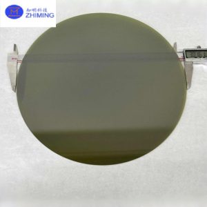
12-Inch 300 mm 4H-SiC Wafer, 750 ± 25 μm
Large-diameter silicon carbide wafer based on the reference listing for 300 mm / 12-inch research-grade substrates. Polytype, conductivity, orientation, thickness, resistivity, defect…
View specifications →SiC substrate formats for power electronics, RF, epitaxy, and device development.
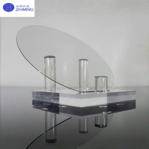
Large-diameter silicon carbide wafer based on the reference listing for 300 mm / 12-inch research-grade substrates. Polytype, conductivity, orientation, thickness, resistivity, defect…
View specifications →
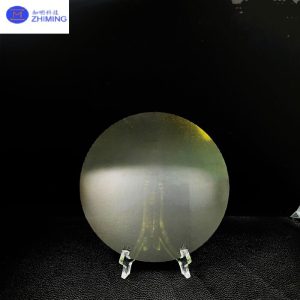
High-purity semi-insulating silicon carbide wafer listed in a 4-inch, 350 μm example for AR-glass and semiconductor development. Confirm resistivity, polytype, surface finish,…
View specifications →
8-inch SiC epitaxial wafer option for power-device and semiconductor development. Specify substrate polytype, conductivity, epi stack, layer thickness, doping, and inspection requirements.
View specifications →Share your material, dimensions, tolerances, quantity, and target date. Our team will review the requirements and respond.