
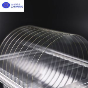
BF33 Borosilicate Glass Substrate for MEMS & Optics
BF33 borosilicate glass substrate listed for semiconductor, MEMS, and optical applications. Specify wafer size, thickness, surface finish, edge profile, and bonding or…
View specifications →Selected glass, compound, and thermal-management substrates for semiconductor, MEMS, photonics, and advanced packaging projects.
BF33 borosilicate glass substrate listed for semiconductor, MEMS, and optical applications. Specify wafer size, thickness, surface finish, edge profile, and bonding or…
View specifications →
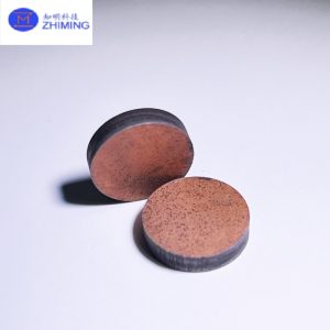
Diamond-copper composite option for high-thermal-conductivity and tailored-expansion designs. Specify composite architecture, dimensions, target thermal performance, test method, and interface requirements.
View specifications →
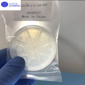
GaN epitaxy template on sapphire listed in 2-, 4-, 6-, and 8-inch formats. Specify wafer diameter, sapphire orientation, GaN/AlN layer structure, thickness,…
View specifications →Share your material, dimensions, tolerances, quantity, and target date. Our team will review the requirements and respond.